SMPS (Switched Mode Power Supply) design is becoming less common in electronics design with integrated magnetics module solutions becoming ever better and smaller. Those that do make their own SMPS designs have to consider cost, space and EMC. In this short series of articles, we want to give you some guidelines on several aspects of buck, boost and buck/boost SMPS designs so that you will be able to choose, design and integrate one into your designs without problems.
PART 4: SMPS Component Placement
Missed part 1, 2 and 3? No problem, here’s the link to part 1, the link to part 2 and the link to part 3.
Where do the currents flow?
The key to any SMPS design is a proper PCB layout: it enables SMPS accuracy, stability, and EMC performance. The main challenge is to route the fastest-changing currents currents in such a way as to minimize the loops, which results in minimized emissions. But where do these currents flow?
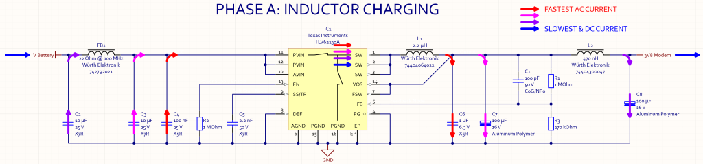
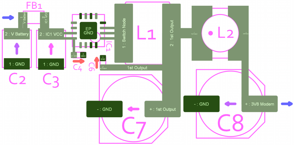
To explain this, let’s take a look at our example buck converter. Its switching cycle has two phases. In phase A, the converter activates the top switch to pass current from the input pin to the switch node pin. This (rising) current flows through the inductor and charges the output capacitors. Due to their specific at various frequencies, the fastest AC currents will flow through the smallest capacitors.
In phase B, the converter activates the bottom switch and the inductor discharges into the output capacitors. Again, the fastest AC currents will flow through the smallest capacitors.
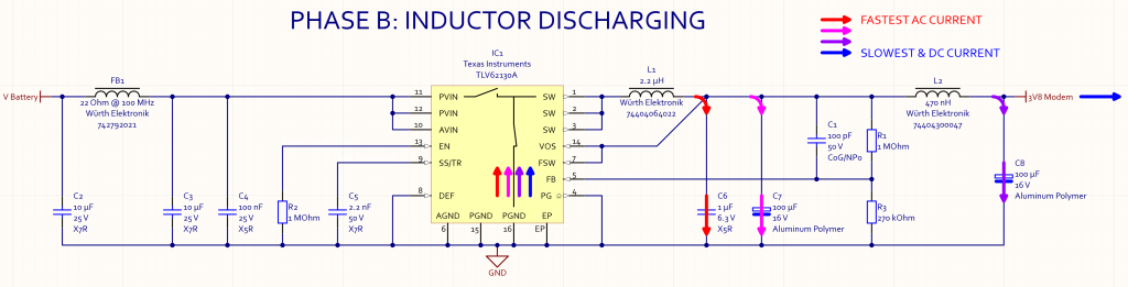
Since the fastest current changes run through C4 and C6, these should be placed as close as possible to IC1. C3 and C7 have second priority, followed by FB1, L2, C2, and C8.
What is “as close as possible”?
Electrical currents will follow the path of least resistance. This is easy to comprehend in DC current situations. AC currents, however, will follow the path of least impedance. Multiple effects influence the flow of high frequency AC currents, such as characteristic impedance and skin effect.
Opinions differ on how this should impact PCB design. Should you use vias at all? Should you opt for a topology with signals on the top layer and a ground plane beneath them, or do you route everything on one layer? In my opinion, it totally depends on the choice of design technology – and personal preference.
Everyone has their own approach, be that scientific or intuitive. At the end of the day, you cannot tamper with the laws of nature. The proof of the pudding is in the eating and performance measurements will reveal whether you made the right choices or not.
Component Placement
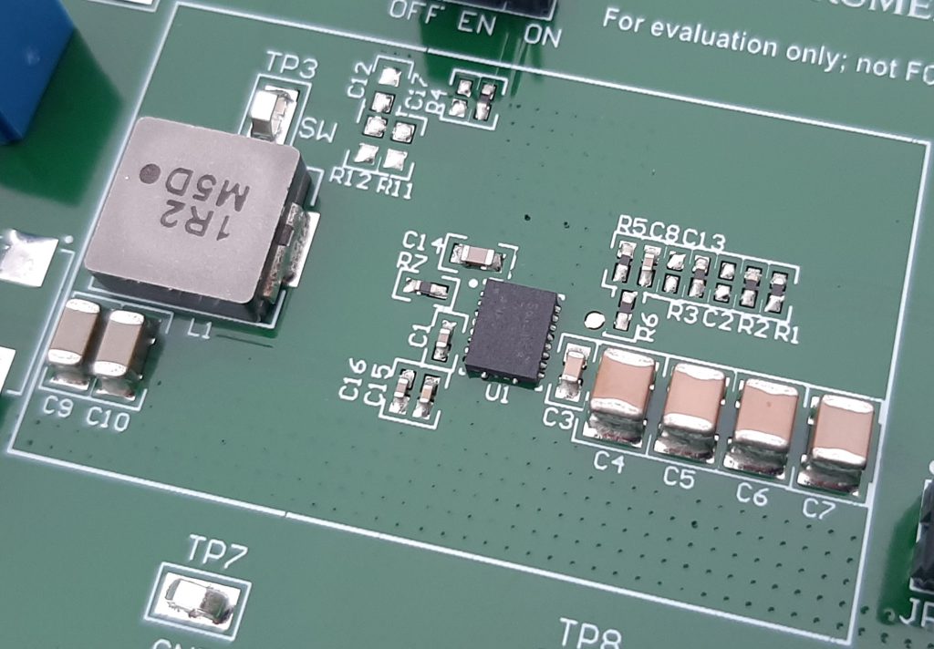
After a bit of shoving around components, I, for one, came up with the placement shown below. The connections are indicative, not definitive. Furthermore, the ground net is not routed but highlighted.
Notice how the ground connections of C4, C6 and IC1 are close to one another. The ground connections of C3, C7 and IC1 form a larger loop and those of C2, C8 and IC1 form an even bigger loop.
To summarize, the faster the AC current in a path changes, the smaller the loop area of that net on the PCB should be. .
Other considerations for component placement
The voltage on the switching node of the regulator constantly switches between the voltage on net IC1 VCC (phase A) and ground (phase B). At every switchover, the voltage changes very fast, causing emissions. The switching node should be made as small as possible to minimize these emissions.
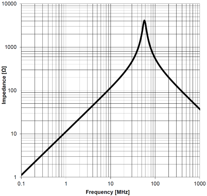
Some people argue that the inductance of L1 limits the rate at which the current through L1 changes, rendering the routing of currents in small loops unnecessary. After all, L1 limits the rate of current change: that is what inductance does. But that claim only holds as long as the inductor is actually an inductor. In this design, L1 has a self-resonant frequency of approximately 60 MHz. Above this frequency, the inductor becomes more and more capacitive, allowing higher frequencies to pass.