SMPS (Switched Mode Power Supply) design is becoming less common in electronics design with integrated magnetics module solutions becoming ever better and smaller. Those that do make their own SMPS designs have to consider cost, space and EMC. In this short series of articles, we want to give you some guidelines on several aspects of buck, boost and buck/boost SMPS designs so that you will be able to choose, design and integrate one into your designs without problems.
Part 3: Example SMPS Schematic
Missed part 1 and 2? No problem, here’s the link to part 1 and the link to part 2.
SMPS Considerations
A 3.8 V SMPS is needed for powering a GPRS modem. The modem is powered on once a day to communicate data and is then switched off again. The available supply voltage is anything between 10 … 16 VDC. The SMPS should be efficient at loads around 300 mA and should be able to supply 2 A at least. The output ripple should also be very low; 50 mVPK-PK up to 200 kHz, 10 mVPK-PK from 200 kHz to 400 kHz and 2 mVPK-PK from 400 kHz onwards.
Because the output voltage is always lower than the input voltage, it is obvious that we want to use a buck type converter. We want to be able to switch the SMPS on and off, so an enable input would be nice. If the regulator would not have an enable input, we would have to add an external switch for the regulator.
The requirement for efficient power conversion means that we want to use lower loss inductors and capacitors than the regulator has been specified with. The efficiency numbers that are mentioned in the data sheet are usually taken from an evaluation kit, leaving room for improvement by selecting better inductors and capacitors. This is also necessary to comply with the output ripple voltage requirement.
Because the modem is not powered continuously, quiescent current consumption is a lesser concern than shutdown current and efficiency. The shutdown current is drawn whenever the product is switched on, effectively 24/7 in most cases. A shutdown current of 100 µA consumes 8.64 J in 24 hours, enough to deliver 300 mA during 29 seconds.
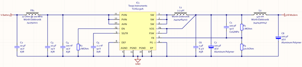
I am a lazy guy. Whenever I am looking for an SMPS IC, my go-to place is the Power Management section of the Texas Instruments website. It has a comprehensive product table with many filtering options. I input the numbers for VIN,MIN , VIN,MAX , IOUT,MAX , VOUT,MIN , VOUT,MAX , IQ and select the “Enable” feature. Then I sort the results on price, lowest price first. At the time of writing this article, the TLV62130(A) came out on top.
The TLV62130(A) buck regulator with integrated switches is ±90 % efficient at 300 mA output current.
The switching frequency of the TLV62130(A) can be set to 2.5 MHz or 1.25 MHz. Though using 2.5 MHz is tempting for noise filtering, the efficiency of the regulator would drop to 85 %, which would be a serious efficiency loss.
To further improve efficiency and support high output currents, a low ESR (14 mOhm) switching inductor is selected. The inductor in the second filter stage has an ESR of 10 mOhm. For lowest output noise, two aluminum polymer output capacitors have been selected with a worst case ESR of 20 mOhm, which is pretty amazing for an electrolytic capacitor. The relatively high leakage current of these capacitors may reduce overall efficiency by 0.3 %, but their superior filtering capabilities due to the low ESR is decisive in this case.
Calculations
The TLV62130(A) datasheet mentions a couple of formulas for calculating output voltage, inductor ripple and peak current, soft start capacitor, loop stability, etc. I usually put these equations in an Excel sheet to have an overview of the intended operating values of the solution.
Input Filter
During normal operation where 300 mA of output current is drawn, the input current will be 127 mA or less. Because of this, the input filter does not need to be bulky or powerful. The ripple voltage at the input of the regulator is kept below ±125 mVPK-PK, even in worst case conditions.
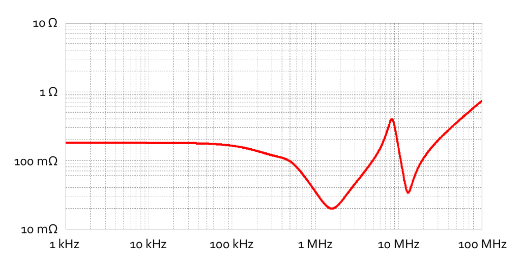
The graph shows a simulation of the impedance that the TLV62130(A) sees on its input. It includes simple RLC models for capacitors, a simple RL model for the ferrite bead and inductance for PCB traces. Estimating the latter can be done by using the Saturn PCB Toolkit.
Because the ferrite bead has little inductance no noticeable impedance peak is present in the lower frequency region. If the impedance peak at 8.3 MHz does not feel right, we could add a 1 µF capacitor to the input filter to keep the impedance below 100 mOhm from 400 kHz to 25 MHz. The 100 nF capacitor will facilitate high-frequency PCB routing, as we will see later.
Inductor
In this case, the inductor current capability is nothing to worry about. Even at the high side switch current limit (4.2 A), the inductance is less than 5 % down. This is a bonus from selecting a low ESR inductor for the switching inductor. The power loss in the inductor is only 56 mW at 2 A output current. The SRF (Self-Resonant Frequency) of the inductor is almost 50 times the switching frequency.
The ripple current in the switching inductor is rather high at 1.5 APK-PK. It would have been nice to be able to use a higher value inductor, but the TLV62130(A) does not allow for such high inductor values due to loop stability. The high ripple current combined with the fact that the inductor is a semi-shielded inductor could have an adverse effect on the EMC performance. If this would be the case, a fully shielded inductor should be selected.
Output Filter
The output filter is comprised of two stages to meet the strict output noise requirements. The selected output capacitors have ESR ratings around those of MLCC capacitors and will achieve good ripple and noise attenuation. The capacitor values are chosen to be within the maximum capacitive load that the regulator allows for. The 1 µF capacitor will facilitate high-frequency PCB routing, as we will see later.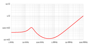
The continuous rise of the output impedance from 1 MHz is caused by the ESL of the second filter stage capacitor and needs to be compensated for. This is done by the decoupling capacitors that are placed locally to the GPRS modem. This local decoupling also reduces the load switching frequency seen by the regulator.